
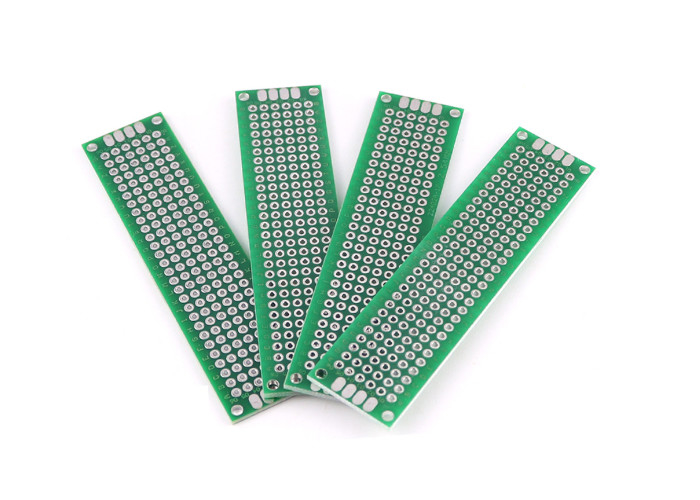
Double Sided Universal Board for Student Welding Experiments One Minimum Aperture
-
Highlight
Double Sided Universal Board
,Student Welding Experiments Universal Board
,One Minimum Aperture Universal Board
-
Character ColorNothing
-
Number Of LayersTwo
-
Special CraftsmanshipCopper Hole 25um
-
Solder Mask CoverageThrough Hole Cover Oil
-
Minimum ApertureOne
-
ImpedanceNo
-
Surface Treatment Of Solder PadsLead Spray Tin
-
Place of OriginChina
-
Model NumberDouble sided universal board, perforated board, universal board, student welding experimental board
-
Minimum Order QuantityNegotiate
-
PriceNegotiate
-
Packaging DetailsCustom packaging
Double Sided Universal Board for Student Welding Experiments One Minimum Aperture
The pictures, models, parameters and other relevant information displayed in the product are for reference only. If you are searching for products related to fields such as electronic components, precision components, office automation, and factory automation, or if you need customized products in this field. Welcome to contact us through the consultation form, telephone or any way you find convenient. We will reply to you as soon as possible. We always adhere to the purpose of striving for the best to provide you with the highest quality service. We look forward to establishing a friendly and stable cooperative relationship with you.
Product Description:
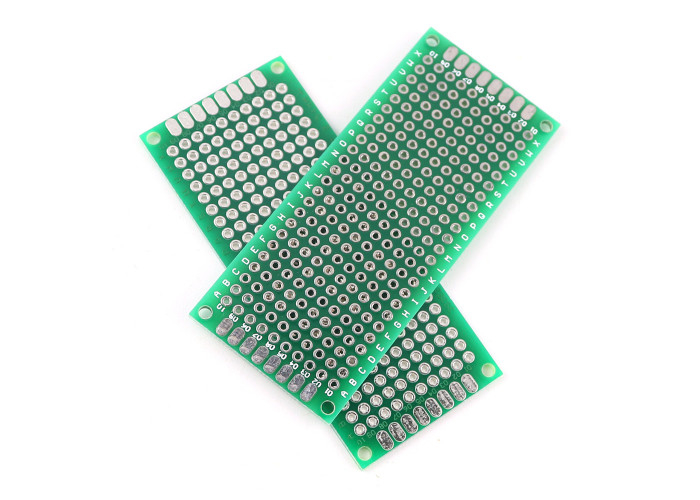
As a multifunctional double-sided universal board with holes, this product has become an ideal choice for students, electronics enthusiasts, and product developers due to its flexible design capabilities, low cost, and convenient usage. Its standard IC spacing, double-sided design, and wide applicability enable it to play an important role in various electronic design scenarios.
Technical Parameter:
| Outer copper thickness | 1oz |
| Surface treatment of solder pads | Lead spray tin |
| Board options | Flame retardant |
| Forming method | Mechanical Forming |
| base material | FR-4 |
| Specification and size | 2×8,3×7cm,4×6cm,5×7cm,6×8cm,7×9cm,8×12cm,9×15cm |
| Testing method | Engineering testing rack |
| Solder mask color | green |
![]()
Applicable scenarios:
Student education: widely used in experimental courses for students majoring in electronic engineering, computer science, etc., as a welding practice and teaching tool.
Electronic Design Competition: Due to its rapid prototyping ability, it has become the preferred material for student electronic design competitions.
Electronic enthusiasts: Support electronic enthusiasts in circuit design, innovative experimentation, and DIY projects.
Initial stage of product development: used for prototype validation and testing during the initial stage of product development.
Product Function:
Flexible wiring: Users can freely wire according to their needs to achieve various electronic circuit designs.
Component installation: Supports the insertion and installation of various standard electronic components without the need for customized PCB boards.
Rapid prototyping: greatly shortens the process from design to physical production and improves development efficiency.
Cost effectiveness: Compared to professional PCB plate making, it has lower costs and is suitable for bulk procurement and experimental use.
Support and Services
- 24/7 customer service support to answer any questions.
- Expert advice on product selection and troubleshooting.
- Detailed product information and training materials.
- Full warranty and repair services.
- Product updates and upgrades.
Packing and Shipping
Double sided universal board, perforated board, universal board, student soldering experimental board, PCB circuit board is packaged and shipped in a cardboard box that is designed to keep the product safe and secure during transit. The box has a custom-sized insert to fit the product securely, and is sealed with tape. Inside the box, the product is wrapped in bubble wrap and foam padding to provide additional cushioning and protection. A packing slip and any promotional materials are included in the package.The package is then shipped via a reliable carrier such as UPS or FedEx. Tracking information is provided to the customer to follow the package's progress. Delivery time will vary depending on the chosen shipping method and destination.
The package is then shipped via a reliable carrier such as UPS or FedEx. Tracking information is provided to the customer to follow the package's progress. Delivery time will vary depending on the chosen shipping method and destination.
![]()
Our products are sold all over the world, you can rest assured.